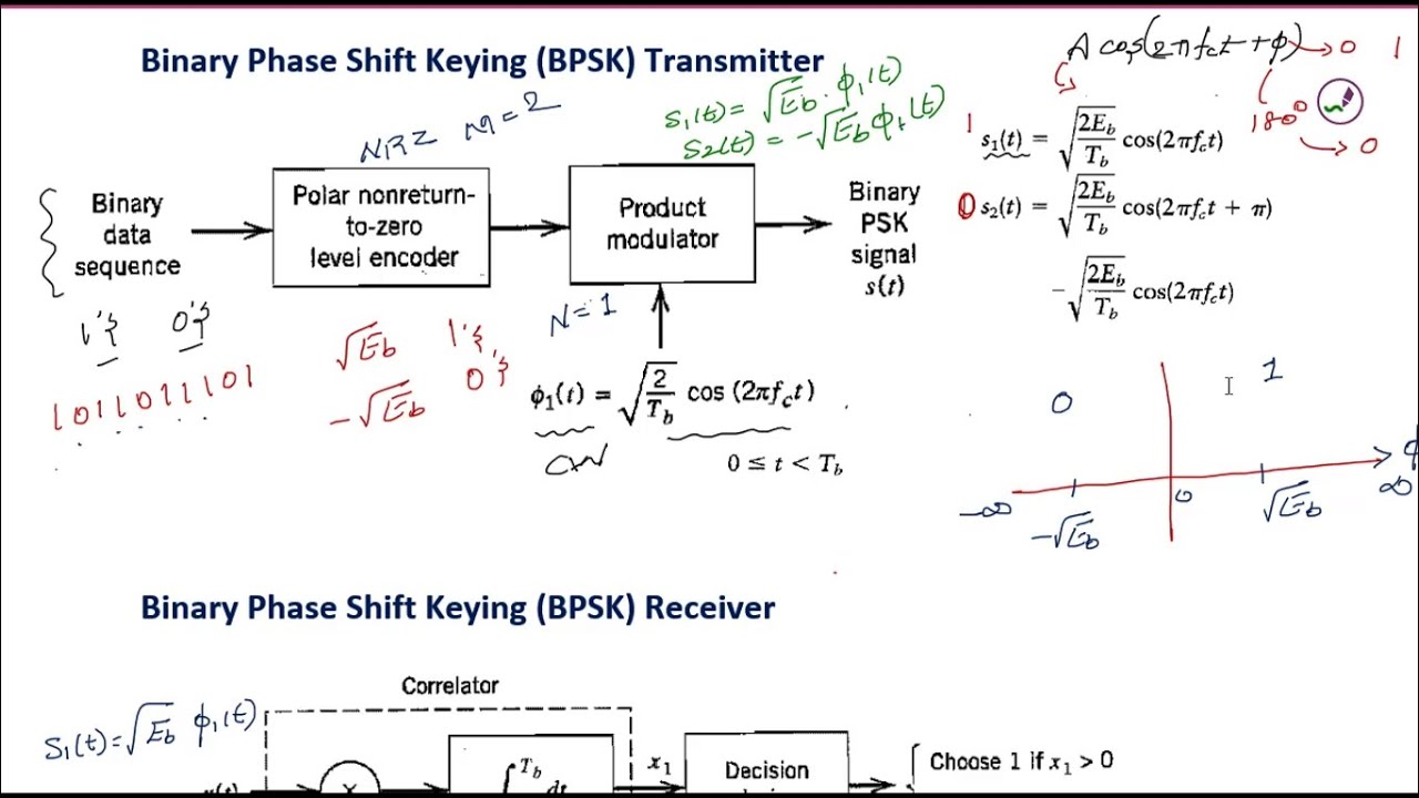
Block Diagram Of Bpsk Modulator
Block diagram of qpsk modulator. Qpsk modulator Bpsk modulators modulator iq
Block diagram of typical BPSK demodulation schemes using carrier
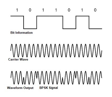
Binary phase shift keying Rf modulator connection diagram Bpsk demodulation transmitter modulation keying phase binary shift matlab output figure gaussianwaves voltage bits represented carrier oscillator frequency multiplying negative
Bpsk modulator cmos
Block diagram of the proposed bpsk demodulation scheme.Bpsk modulator implemented modulation spectrum spread block Psk modulation demodulation demodulator bpsk qpskBpsk block simulink diagram phase keying shift modulator transmitter signal processing blocks library using part.
Bpsk receiver demodulation modulation matlab explanation code completeBpsk transmitter and receiver Bpsk modulator and its co-simulation block using system generatorTransmitter modulator rf bpsk supply 2ghz.
Bpsk modulation representation frequency corresponding
Block diagram of the spread spectrum and bpsk modulation systemBpsk diagram demodulation shift phase keying binary digital detector theory data experiment fig set Bpsk modulator fpgaBlock diagram of the bpsk transceiver.
Bpsk system with block diagramBpsk modulator Bpsk transmitter keying binaryDpsk modulation,dpsk demodulation,differential phase shift keying.

Block diagram of the modified reflection-type modulators. (a) bpsk
4.: schematic representation of normal bpsk modulation. the left partBpsk modulation and demodulation- complete matlab code with explanation Bpsk demodulation schemeBpsk demodulation carrier costas squaring.
Bpsk modulation phase diagram block system svg file gps ru represented basis function single using may wikimedia commonsLowpass filter Bpsk modulation and demodulation- complete matlab code with explanationBpsk transceiver.

Block diagram of typical bpsk demodulation schemes using carrier
Figure 1 from a cmos direct-digital bpsk modulator using an activeFigure 3 from simulation and implementation of a bpsk modulator on fpga Dpsk demodulator demodulation phase modulation differential keying shift using rfwireless basicsBpsk modulator modulation demodulation matlab code explanation implementation complete.
.


lowpass filter - Block diagram of M-PSK modulation and demodulation

Figure 1 from A CMOS Direct-Digital BPSK Modulator Using an Active

Rf Modulator Connection Diagram - A Bpsk Modulator For 2ghz To 12ghz
BPSK System with Block Diagram - Electronics and Communication Study

4.: Schematic representation of normal BPSK modulation. The left part

Block diagram of the proposed BPSK demodulation scheme. | Download

Block Diagram of QPSK Modulator. | Download Scientific Diagram

Block diagram of typical BPSK demodulation schemes using carrier
